| CPC G06F 3/0659 (2013.01) [G06F 1/06 (2013.01); G06F 3/0611 (2013.01); G06F 3/0656 (2013.01); G06F 3/0679 (2013.01); G11C 16/10 (2013.01); G11C 16/26 (2013.01); G11C 16/32 (2013.01); G11C 16/0483 (2013.01)] | 17 Claims |
|
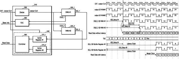
1. A memory system comprising:
a memory controller configured to transmit, to a host device, read data according to a first clock, in response to read command received from the host device; and
a memory device including,
a first NVM,
a second NVM, and
an interface circuit connected between the memory controller and the first NVM and the second NVM, the interface circuit configured to,
receive, from the memory controller, the first clock, and to generate and transmit, a second clock which is divided from the first clock based on a number of NVMs, to each of the first NVM and the second NVM,
receive, at a first time, a first data strobe signal generated by the first NVM,
receive, at a second time, a second data strobe signal generated by the second NVM,
identify a skew based on the first time and the second time,
identify a first time delay associated with outputting data from the first NVM and a second time delay associated with outputting data from the second NVM based on the skew, and
generate and transmit, to the memory controller, the read data by,
temporarily storing first divided read data received from the first NVM and second divided read data received from the second NVM in a first buffer register and a second buffer register, respectively,
outputting the first divided read data from the first NVM based on the first time delay and the second divided read data from the second NVM based on the second time delay,
combining the first divided read data that was output based on the first time delay and the second divided read data that was output based on the second time delay to generate the read data, and
transmitting the read data to the memory controller.
|