| CPC G06F 3/0443 (2019.05) [G06F 3/0412 (2013.01); G06F 3/0448 (2019.05)] | 15 Claims |
|
1. A display device comprising:
pixel electrodes arranged along a first direction and a second direction perpendicular to the first direction, the pixel electrodes including a first pixel electrode and a second pixel electrode that are adjacent to each other in the second direction, and a third pixel electrode that is adjacent to the second pixel electrode in the first direction;
a common electrode overlapping the pixel electrodes such that a first insulating film is between the common electrode and the pixel electrodes;
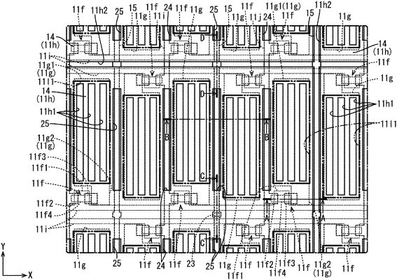
a line extending in the first direction and contacted with the common electrode, the line including a first side edge and a second side edge that is an opposite side edge from the first side edge with respect to the second direction, the first side edge and the second side edge extending in the first direction;
image signal lines extending in the first direction to transmit image signals to the pixel electrodes, the image signal lines including a first image signal line opposite the first side edge of the line and a second image signal line opposite the second side edge of the line;
scan lines extending in the second direction to transmit scan signals, the scan lines including a first scan line and a second scan line, the first scan line and the second scan line being arranged at an interval in the first direction, a section of the first scan line and a section of the second scan line being in a space between the second pixel electrode and the third pixel electrode;
a first gate electrode protruding from the first scan line in the first direction to be away from the interval;
a second gate electrode protruding from the second scan line in the first direction to be away from the interval; and
thin film transistors coupled to each of the pixel electrodes, the image signal lines, and the scan lines, the thin film transistors including a first thin film transistor coupled to the first pixel electrode, a second thin film transistor coupled to the second pixel electrode, and a third thin film transistor coupled to the third pixel electrode, wherein
the first pixel electrode is between the line and the first image signal line, and the second pixel electrode and the third pixel electrode are between the line and the second image signal line.
|