| CPC G06F 3/0412 (2013.01) [G02F 1/13338 (2013.01); G02F 1/134363 (2013.01); G02F 1/1368 (2013.01); G06F 3/0445 (2019.05); G06F 3/0446 (2019.05); G02F 1/133553 (2013.01); G02F 2201/44 (2013.01); G06F 2203/04108 (2013.01)] | 5 Claims |
|
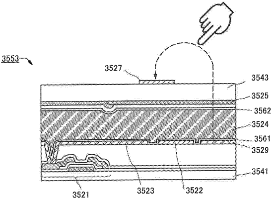
1. An input/output device comprising:
a touch sensor, the touch sensor comprising:
a first electrode over a substrate; and
a second electrode under the substrate;
a light-emitting element under the substrate, the light-emitting element comprising:
a third electrode;
a fourth electrode; and
a layer containing a light-emitting material; and
an insulating layer between the substrate and the fourth electrode,
wherein a capacitor is formed between the first electrode and the second electrode,
wherein the insulating layer is in contact with a surface of the fourth electrode and a surface of the second electrode,
wherein the third electrode is a pixel electrode,
wherein the second electrode comprises a same material as the fourth electrode,
wherein the second electrode is isolated from the fourth electrode,
wherein the second electrode is on a same layer as the fourth electrode, and
wherein a part of the third electrode overlaps with a part of the second electrode.
|