|
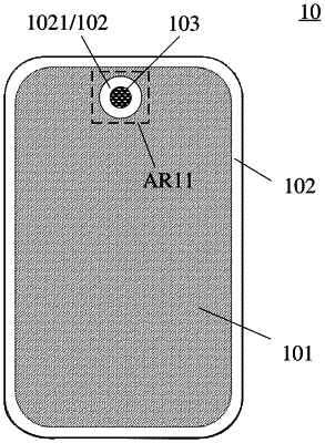
1. An electronic substrate, comprising a first functional region, a second functional region, and a peripheral region surrounding the first functional region, wherein the first functional region comprises an opening, and the second functional region is in the opening; the peripheral region comprises an opening peripheral region at least partially in the opening, the opening peripheral region at least partially surrounds the second functional region and is between the second functional region and the first functional region; the electronic substrate comprises a base substrate and a detection trace structure on the base substrate, the detection trace structure is along an edge of the peripheral region, a first end of the detection trace structure is configured to be connected to a detection signal source, and a second end of the detection trace structure is configured to be connected to a detection circuit; the detection trace structure comprises a first conductive trace and a second conductive trace in the opening peripheral region and at least partially surrounding the second functional region, the first conductive trace and the second conductive trace respectively extend from a first position along an edge of the second functional region in a reverse direction and respectively partially surround the second functional region, and the first conductive trace and the second conductive trace are spaced apart from each other in the first position, a contour of an orthographic projection of the first conductive trace and an orthographic projection of the second conductive trace on the base substrate at least partially surround an orthographic projection of the second functional region on the base substrate, so that the orthographic projection of the second functional region on the base substrate is in a region enclosed by the orthographic projection of the first conductive trace and the orthographic projection of the second conductive trace on the base substrate; and the electronic substrate comprises a first electrode layer, an insulating layer and a second electrode layer that are sequentially stacked on the base substrate, the first conductive trace is in the first electrode layer and the second conductive trace is in the second electrode layer, and the first conductive trace and the second conductive trace are spaced apart from each other in a direction perpendicular to the base substrate by the insulating layer and electrically connected to each other at a second position; and wherein the opening peripheral region comprises a first cofferdam region, a second cofferdam region and a spacing region; the first cofferdam region at least partially surrounds the first functional region, the spacing region at least partially surrounds the first cofferdam region, and the second cofferdam region at least partially surrounds the spacing region; the electronic substrate comprises a first cofferdam structure and a second cofferdam structure, the first cofferdam structure is in the first cofferdam region and the second cofferdam structure is in the second cofferdam region; the first conductive trace is at least between the second cofferdam region and the second functional region, the second conductive trace is at least between the second cofferdam region and the second functional region; and in the direction perpendicular to the base substrate, the first conductive trace and the second conductive trace are on a side of the first cofferdam structure and the second cofferdam structure away from the base substrate.
|
