| CPC G06F 15/8007 (2013.01) [G06F 9/30036 (2013.01); G06F 9/30043 (2013.01); G06F 9/30112 (2013.01)] | 42 Claims |
|
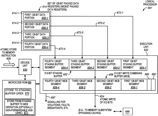
1. A processor comprising:
a plurality of caches;
decode circuitry to decode an instruction, the instruction to provide information to address a source memory location and to provide information to address a destination memory location;
execution circuitry coupled with the decode circuitry, the execution circuitry to perform operations corresponding to the instruction, including to atomically store first data, including data loaded from the source memory location, to the destination memory location; and
a status register coupled with the execution circuitry, wherein status information is to be stored in a bit of the status register, the status information indicative of whether the first data has been stored to the destination memory location.
|