US 12,007,930 B2
Low voltage drive circuit with drive sense and methods for use therewith
Richard Stuart Seger, Jr., Belton, TX (US); Daniel Keith Van Ostrand, Leander, TX (US); Gerald Dale Morrison, Redmond, WA (US); and Timothy W. Markison, Mesa, AZ (US)
Assigned to SigmaSense, LLC., Wilmington, DE (US)
Filed by SigmaSense, LLC., Wilmington, DE (US)
Filed on May 17, 2023, as Appl. No. 18/319,283.
Application 18/319,283 is a continuation of application No. 18/149,932, filed on Jan. 4, 2023, granted, now 11,693,811.
Application 18/149,932 is a continuation of application No. 17/663,947, filed on May 18, 2022, granted, now 11,580,047, issued on Feb. 14, 2023.
Application 17/663,947 is a continuation of application No. 17/444,016, filed on Jul. 29, 2021, granted, now 11,366,780, issued on Jun. 21, 2022.
Application 17/444,016 is a continuation of application No. 17/141,531, filed on Jan. 5, 2021, granted, now 11,151,072, issued on Oct. 19, 2021.
Application 17/141,531 is a continuation of application No. 16/884,339, filed on May 27, 2020, granted, now 10,915,483, issued on Feb. 9, 2021.
Application 16/884,339 is a continuation in part of application No. 16/854,379, filed on Apr. 21, 2020, granted, now 10,733,133, issued on Aug. 4, 2020.
Application 16/854,379 is a continuation in part of application No. 16/246,772, filed on Jan. 14, 2019, granted, now 10,684,977, issued on Jun. 16, 2020.
Prior Publication US 2023/0289314 A1, Sep. 14, 2023
This patent is subject to a terminal disclaimer.
Int. Cl. G06F 13/40 (2006.01); H04L 7/04 (2006.01); H04L 12/40 (2006.01); H03F 3/45 (2006.01); H04L 25/02 (2006.01)
CPC G06F 13/4072 (2013.01) [H04L 7/04 (2013.01); H04L 12/40045 (2013.01); G06F 2213/0016 (2013.01); H03F 3/45 (2013.01); H04L 25/0282 (2013.01)] 20 Claims
OG exemplary drawing
 
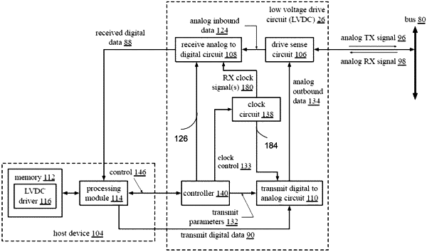
1. A low voltage drive circuit (LVDC) comprises:
a transmit digital to analog circuit configured to convert transmit digital data into analog outbound data by:
generating an oscillating component, via an output limited digital to analog converter, wherein the oscillating component is generated in accordance with the transmit digital data as an oscillation within a first frequency range having oscillation characteristics, wherein magnitude of the oscillation is limited to a range that is less than a difference between magnitudes of power supply rails; and
combining a DC component with the oscillating component to produce the analog outbound data; and
a drive sense circuit configured to:
convert the analog outbound data into an analog transmit signal;
drive the analog transmit signal onto a bus, wherein the analog outbound data is represented within the analog transmit signal as variances in loading of the bus within the first frequency range;
receive an analog receive signal from the bus by isolating the analog receive signal from the analog transmit signal; and
recover analog inbound data from the analog receive signal as variances in loading of the bus within a second frequency range, wherein the first frequency range is different from the second frequency range.