| CPC G06F 11/2094 (2013.01) [G11C 16/0483 (2013.01); G06F 2201/85 (2013.01); G11C 16/26 (2013.01)] | 20 Claims |
|
1. A memory device comprising:
a processor;
a memory, storing instructions, which when executed, causes the processor to perform operations comprising:
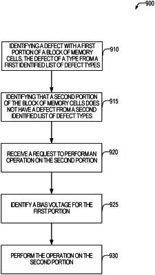
identifying that a first deck of a block of three-dimensional NAND has a defect of a type from an identified list of defect types;
identifying that a second deck of the block does not have a defect from the identified list of defect types;
testing the second deck to determine if it meets at least one quality criterion;
responsive to determining that the second deck meets at least one quality criterion, marking the second deck as salvageable;
receiving a memory device request;
identifying a bias voltage for the first deck of the block; and
servicing the memory device request serviced using NAND cells in the second deck, the servicing the memory device request comprising disabling the first deck during the servicing by applying the bias voltage to word lines of the first deck.
|