| CPC G06F 1/189 (2013.01) [G02F 1/13458 (2013.01); G06F 1/20 (2013.01); G09G 3/20 (2013.01); H05K 1/0209 (2013.01); H05K 7/20963 (2013.01); G09G 2310/0275 (2013.01); H05K 1/147 (2013.01)] | 20 Claims |
|
1. A display device comprising:
a display panel;
a data driver which transmits a data voltage to the display panel;
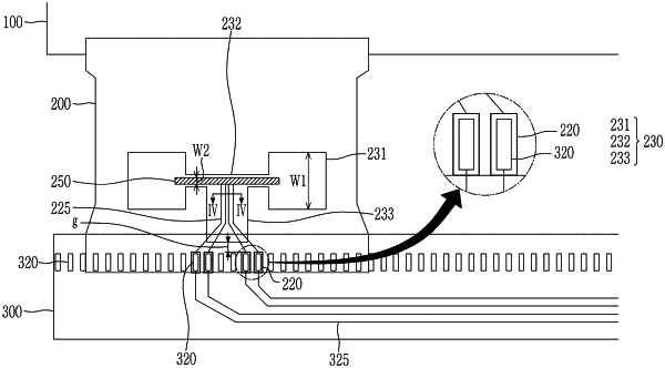
a first flexible printed circuit board attached to the display panel and including an input side wiring electrically connected to the data driver;
a first printed circuit board (PCB) electrically connected to the input side wiring to transmit a high-speed driving signal to the data driver; and
a metal tape overlapping the input side wiring in a plan view and attached on the first flexible printed circuit board,
wherein the metal tape comprises
a metal layer;
a first adhesive layer disposed between the metal layer and the first flexible printed circuit board;
a reinforcement layer; and
a second adhesive layer disposed between the metal layer and the reinforcement layer.
|