| CPC G03F 7/2022 (2013.01) [G03F 1/42 (2013.01); G03F 7/2004 (2013.01); G03F 7/70625 (2013.01); G03F 7/7085 (2013.01); G03F 9/7065 (2013.01)] | 20 Claims |
|
1. A method for semiconductor processing, the method comprising:
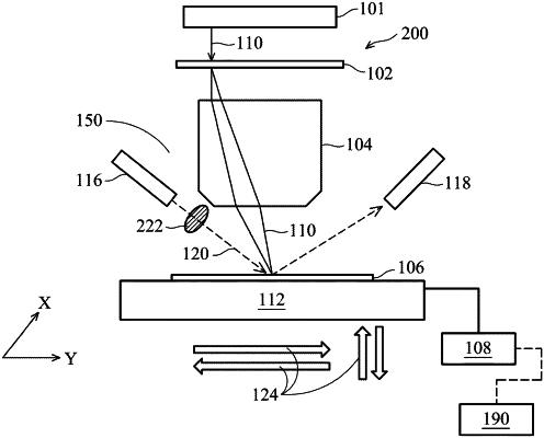
providing beams of light from an emitter, wherein the beams of light have multiple wavelengths;
passing the beams of light have multiple wavelengths through a polarizer;
providing the beams of light that have passed through the polarizer to a substrate via at least one optical fiber including multiple zones, each of the multiple zones including strands of optical fibers, a material of the strands of optical fibers of a zone being different from the material of the strands of optical fibers of a different zone, the substrate include materials having different transmittance with respect to the beams of light having the multiple wavelengths;
collecting reflected light of the beams of light at a receiver, the reflected light being reflected off of the substrate;
determining a variation of height of the substrate based on the collected reflected light; and
aligning the substrate with an optical focusing module in response to the determined variation of height of the substrate.
|