| CPC G03F 1/24 (2013.01) [H01L 21/0332 (2013.01); H01L 21/0337 (2013.01)] | 34 Claims |
|
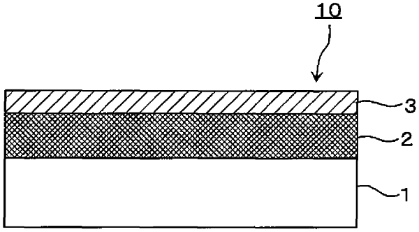
1. A mask blank comprising:
a substrate; and
a hard mask film formed on the substrate, wherein
the hard mask film is a single layer film having a composition gradient portion formed on a surface of the hard mask film that faces away from the substrate and in a region adjacent to the surface,
the hard mask film is made of a material containing chromium, oxygen, and carbon with a total content of chromium, oxygen, and carbon being 95 atomic % or more,
a part of the hard mask film excluding the composition gradient portion has a chromium content of 50 atomic % or more,
a ratio of a carbon content [atomic %] divided by a total content [atomic %] of chromium, carbon, and oxygen in the part of the hard mask film excluding the composition gradient portion is 0.1 or more,
a ratio of a carbon content [atomic %] divided by a total content [atomic %] of chromium and carbon in the part of the hard mask film excluding the composition gradient portion is 0.14 or more, and
a content of nitrogen in the hard mask film is equal to or less than a detection limit value in composition analysis of X-ray photoelectron spectroscopy.
|
|
15. A method of manufacturing a reflective mask using the mask blank according to claim 9, the method comprising:
performing a first dry etching to form a pattern on the hard mask film; and
performing a second dry etching to form a transfer pattern on the absorber film, wherein a mask used for the second dry etching is the hard mask film provided with the pattern.
|
|
17. A method of manufacturing a semiconductor device, comprising exposure-transferring a transfer pattern of a reflective mask onto a resist film on a semiconductor substrate, the reflective mask having been manufactured from the mask blank according to claim 9.
|