| CPC G02F 1/3136 (2013.01) [G02B 6/29331 (2013.01); G02B 6/29355 (2013.01); G02F 1/313 (2013.01); G02B 6/125 (2013.01)] | 8 Claims |
|
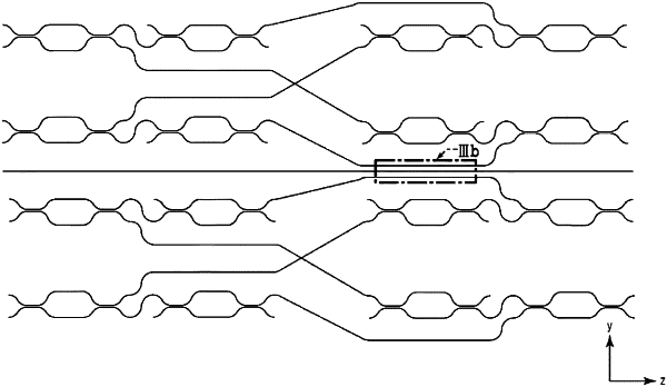
1. An optical signal processing device including a plurality of input optical waveguides, a plurality of output optical waveguides, a plurality of optical waveguide elements arranged between the plurality of input optical waveguides and the plurality of output optical waveguides, and a first connection optical waveguide that connects a first one of the plurality of optical waveguide elements with a first one of the plurality of output optical waveguides, wherein
the connection optical waveguide is positioned closely to a non-connected optical waveguide that is not connected to any of the plurality of input waveguides, any of the plurality of output waveguides, and any of the plurality of optical waveguide elements,
the first connection waveguide is differentiated in propagation constant from the non-connected optical waveguide,
the first connection waveguide is not closely positioned to any of the plurality of input optical waveguides, and
the non-connected waveguide and the first connection optical waveguide are positioned between two of the plurality of optical elements that are not connected to the first connection optical waveguide.
|