US 12,007,656 B2
Display device
Hajime Kimura, Atsugi (JP); and Atsushi Umezaki, Isehara (JP)
Assigned to Semiconductor Energy Laboratory Co., Ltd., Atsugi (JP)
Filed by Semiconductor Energy Laboratory Co., Ltd., Atsugi (JP)
Filed on Nov. 4, 2022, as Appl. No. 17/980,674.
Application 15/711,029 is a division of application No. 15/262,611, filed on Sep. 12, 2016, granted, now 9,798,211, issued on Oct. 24, 2017.
Application 17/980,674 is a continuation of application No. 17/488,398, filed on Sep. 29, 2021, granted, now 11,500,254.
Application 17/488,398 is a continuation of application No. 16/925,535, filed on Jul. 10, 2020, granted, now 11,143,925, issued on Oct. 12, 2021.
Application 16/925,535 is a continuation of application No. 15/991,170, filed on May 29, 2018, granted, now 10,718,986, issued on Jul. 21, 2020.
Application 15/991,170 is a continuation of application No. 15/711,029, filed on Sep. 21, 2017, granted, now 10,007,160, issued on Jun. 26, 2018.
Application 15/262,611 is a continuation of application No. 14/602,876, filed on Jan. 22, 2015, granted, now 9,465,271, issued on Oct. 11, 2016.
Application 14/602,876 is a continuation of application No. 13/021,955, filed on Feb. 7, 2011, granted, now 8,947,337, issued on Feb. 3, 2015.
Claims priority of application No. 2010-028285 (JP), filed on Feb. 11, 2010.
Prior Publication US 2023/0058628 A1, Feb. 23, 2023
Int. Cl. G02F 1/1362 (2006.01); G02F 1/1368 (2006.01); G09G 3/00 (2006.01); G09G 3/36 (2006.01); H01L 27/12 (2006.01); H01L 29/786 (2006.01); G02F 1/1333 (2006.01); G02F 1/1339 (2006.01); G02F 1/1343 (2006.01); G02F 1/167 (2019.01); H01L 29/423 (2006.01)
CPC G02F 1/13624 (2013.01) [G02F 1/136259 (2013.01); G02F 1/136286 (2013.01); G02F 1/1368 (2013.01); G09G 3/006 (2013.01); G09G 3/3648 (2013.01); H01L 27/1225 (2013.01); H01L 27/124 (2013.01); H01L 27/1255 (2013.01); H01L 29/7869 (2013.01); G02F 1/133302 (2021.01); G02F 1/133345 (2013.01); G02F 1/1339 (2013.01); G02F 1/134309 (2013.01); G02F 1/13439 (2013.01); G02F 1/136254 (2021.01); G02F 1/167 (2013.01); G09G 2230/00 (2013.01); G09G 2310/0251 (2013.01); H01L 29/42384 (2013.01)] 3 Claims
OG exemplary drawing
 
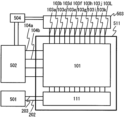
1. A display device comprising:
a pixel portion including a plurality of first transistors; and
a circuit including a plurality of second transistors, the circuit being configured to inspect whether the plurality of the first transistors normally operate or not,
wherein channel formation regions of the plurality of the first transistors and the plurality of the second transistors include oxide semiconductor,
wherein gate electrodes of the plurality of the second transistors are electrically connected to a first wiring,
wherein the first wiring includes at least three lines, and signals are configured to be supplied to the at least three lines at different timings,
wherein source or drain electrodes of the plurality of the second transistors are electrically connected to a second wiring,
wherein a channel width of the plurality of the second transistors is larger than a channel width of the plurality of the first transistors, and
wherein an off-state current per channel width of 1 μm of the plurality of the first transistors and the plurality of the second transistors is 100 aA or less.