| CPC G02F 1/133526 (2013.01) [G02F 1/13363 (2013.01); G02F 1/13439 (2013.01); G02F 2201/121 (2013.01); G02F 2201/123 (2013.01)] | 27 Claims |

|
1. A liquid crystal display device, comprising:
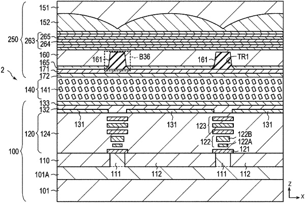
a first substrate that includes a microlens corresponding to each pixel;
a second substrate that faces the first substrate; and
a liquid crystal material layer sandwiched between the first substrate and the second substrate, wherein
a first transparent material layer is in the first substrate and includes a material that has a first refractive index,
a material that has a second refractive index different from the first refractive index is in a portion of the first transparent material layer corresponding to a region between adjacent pixels,
a second transparent material layer is in the second substrate and includes a material that has a third refractive index,
a material that has a fourth refractive index different from the third refractive index is in a portion of the second transparent material layer corresponding to the region between the adjacent pixels,
a third transparent material layer is on the first transparent material layer in the first substrate and includes a material that has a fifth refractive index higher than the second refractive index,
the material that has the second refractive index is embedded in a first groove,
the first groove is in portions of the first transparent material layer and the third transparent material layer corresponding to the region between the adjacent pixels, and
the adjacent pixels include the pixel.
|