US 12,007,636 B2
Manufacturing method for liquid crystal display device
Hideo Tanabe, Mobara (JP); Masaru Takabatake, Mobara (JP); Toshiki Kaneko, Chiba (JP); Atsushi Hasegawa, Togene (JP); and Hiroko Sehata, Ooamishirasoto (JP)
Assigned to Japan Display Inc., Tokyo (JP); and Pansonic Liquid Crystal Display Co., Ltd., Hyogo-Ken (JP)
Filed by Japan Display Inc., Tokyo (JP); and Panasonic Intellectual Property Corporation of America, Torrance, CA (US)
Filed on Oct. 7, 2022, as Appl. No. 17/961,617.
Application 17/961,617 is a continuation of application No. 17/187,945, filed on Mar. 1, 2021, granted, now 11,536,999.
Application 17/187,945 is a continuation of application No. 16/735,388, filed on Jan. 6, 2020, granted, now 10,962,815, issued on Mar. 30, 2021.
Application 16/735,388 is a continuation of application No. 16/161,988, filed on Oct. 16, 2018, granted, now 10,564,459, issued on Feb. 18, 2020.
Application 16/161,988 is a continuation of application No. 15/680,868, filed on Aug. 18, 2017, granted, now 10,133,103, issued on Nov. 20, 2018.
Application 15/680,868 is a continuation of application No. 15/002,453, filed on Jan. 21, 2016, granted, now 9,766,489, issued on Sep. 19, 2017.
Application 15/002,453 is a continuation of application No. 14/679,154, filed on Apr. 6, 2015, granted, now 9,274,364, issued on Mar. 1, 2016.
Application 14/679,154 is a continuation of application No. 14/156,957, filed on Jan. 16, 2014, granted, now 9,025,103, issued on May 5, 2015.
Application 14/156,957 is a continuation of application No. 13/946,700, filed on Jul. 19, 2013, granted, now 8,735,901, issued on May 27, 2014.
Application 13/946,700 is a continuation of application No. 13/568,672, filed on Aug. 7, 2012, granted, now 8,513,701, issued on Aug. 20, 2013.
Application 13/568,672 is a continuation of application No. 13/067,281, filed on May 20, 2011, granted, now 8,377,765, issued on Feb. 19, 2013.
Application 13/067,281 is a continuation of application No. 12/662,961, filed on May 13, 2010, granted, now 7,968,357, issued on Jun. 28, 2011.
Application 12/662,961 is a continuation of application No. 11/802,385, filed on May 22, 2007, granted, now 7,742,113, issued on Jun. 22, 2010.
Claims priority of application No. 2006-160428 (JP), filed on Jun. 9, 2006.
Prior Publication US 2023/0036779 A1, Feb. 2, 2023
Int. Cl. G02F 1/1333 (2006.01); G02F 1/1335 (2006.01); G02F 1/1343 (2006.01); G02F 1/1362 (2006.01); G02F 1/1368 (2006.01); H01L 27/12 (2006.01); H01L 29/786 (2006.01)
CPC G02F 1/133345 (2013.01) [G02F 1/133305 (2013.01); G02F 1/136213 (2013.01); G02F 1/136227 (2013.01); G02F 1/1368 (2013.01); H01L 27/124 (2013.01); H01L 27/1248 (2013.01); H01L 29/78675 (2013.01); G02F 1/133504 (2013.01); G02F 1/133555 (2013.01); G02F 1/134363 (2013.01); G02F 1/13685 (2021.01)] 15 Claims
OG exemplary drawing
 
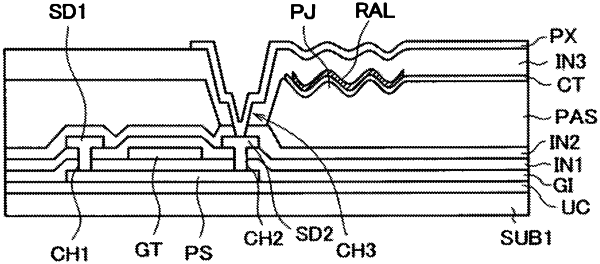
1. A display device comprising:
a substrate;
a first inorganic insulation film above the substrate, having a first hole;
an organic insulation film above the first inorganic insulation film, having a second hole; and
a second inorganic insulation film above the organic insulating film, covering a sidewall of the second hole, and having a third hole, wherein
the organic insulating film is provided between the first inorganic insulating film and the second inorganic insulating film,
each of the first hole and the third hole is located in the second hole, the first hole and the third hole overlap each other in the second hole,
the first inorganic insulation film contacts the second inorganic insulation film without the organic insulation film therebetween inside of the sidewall of the second hole,
a first transparent conductive film is provided above the second inorganic insulating film,
the second inorganic insulating film is provided between the first transparent insulating film and the organic insulating film,
a metal portion is provided between the substrate and the first inorganic insulating film,
the first transparent conductive film is in contact with the metal portion through the first hole and the third hole inside of the sidewall of the second hole, and
the first transparent conductive film has a plurality of slits.