| CPC G02B 6/12019 (2013.01) [G02B 6/132 (2013.01); G02B 6/136 (2013.01); G02B 2006/12061 (2013.01)] | 16 Claims |
|
1. A method of fabricating a photonic integrated circuit (PIC) system, comprising:
lithographically defining a PIC structure on a substrate using a first lithographic patterning technique, the PIC structure comprising:
a plurality of circuit block regions; and
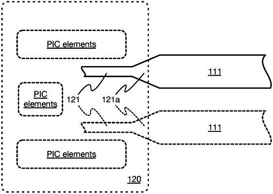
a set of connecting waveguides, each connecting waveguide of the set of connecting waveguides having a first width, and optically coupling respective circuit block regions of the plurality of circuit block regions; and
lithographically defining a photonic circuit block within each circuit block region using a second lithographic patterning technique, each photonic circuit block comprising:
a respective transition waveguide having a second width, less than the first width, and
optically coupled to a corresponding connecting waveguide;
a respective transition feature extending between the respective transition waveguide and the corresponding connecting waveguide, tapering from the first width to the second width; and
a photonic circuit element optically coupled to the respective transition waveguide;
wherein defining each respective transition feature comprises providing a tapered masked feature over each connecting waveguide configured to define each respective transition feature; and
wherein each tapered masked feature has a maximum width greater than the first width, and extends past the first width in both directions.
|