| CPC G02B 3/0006 (2013.01) [G02B 1/115 (2013.01); H04N 23/60 (2023.01); H04N 25/11 (2023.01)] | 26 Claims |
|
1. An image sensor comprising:
a sensor substrate including a first pixel, configured to sense light of a first wavelength, and a second pixel configured to sense light of a second wavelength;
a spacer layer on the sensor substrate, the spacer layer being transparent; and
a color separating lens array on the spacer layer, the color separating lens array being configured to condense the light of the first wavelength incident on the color separating lens array toward the first pixel,
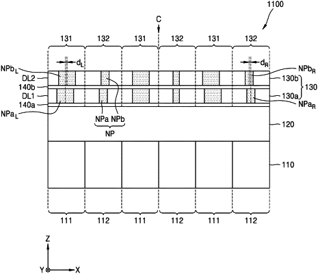
wherein the color separating lens array includes a first lens layer on the spacer layer, a second lens layer on the first lens layer, and a first etch prevention layer between the first lens layer and the second lens layer,
wherein the first lens layer comprises a first pixel region corresponding to the first pixel and a second pixel region corresponding to the second pixel, each of the first pixel region and the second pixel region comprising a plurality of first nanoposts and a first dielectric material layer provided between the plurality of first nanoposts, and
wherein the first etch prevention layer is provided on upper surfaces of the plurality of first nanoposts and an upper surface of the first dielectric material layer.
|