| CPC G01R 31/2894 (2013.01) [G01R 31/2856 (2013.01)] | 21 Claims |
|
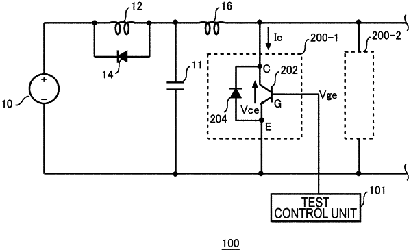
1. A test method of a semiconductor device under test, the test method comprising:
controlling the semiconductor device under test to an on state by inputting a control signal to the semiconductor device under test; and
observing the semiconductor device under test at a time of controlling the semiconductor device under test in the on state to an off state and evaluating the semiconductor device under test,
wherein the semiconductor device under test includes one semiconductor device under test or a plurality of semiconductor devices under test, and
in the controlling to the on state, a length of an on-time for which the one semiconductor device under test or the plurality of semiconductor devices under test are set to the on state is adjusted based on a magnitude of a variation in a delay time of the control signal among a plurality of regions in one of the one or the plurality of semiconductor devices under test or among the plurality of semiconductor devices under test.
|