| CPC G01R 31/2831 (2013.01) [H01L 22/34 (2013.01)] | 20 Claims |
|
1. A wafer, comprising:
a die;
a scribe line adjacent to the die; and
a test circuit adjacent to the scribe line, the test circuit including:
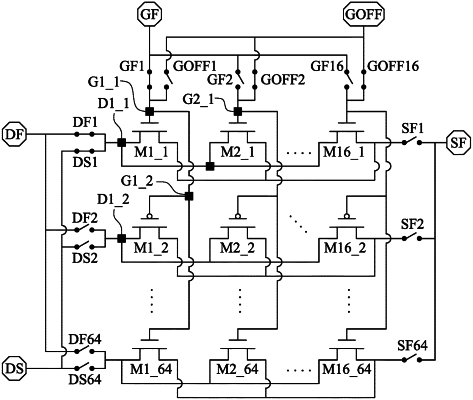
a first switch configured to turn on or turn off a first set of devices under test (DUTs) arranged in a first column;
a second switch configured to turn on or turn off a second set of DUTs arranged in a second column;
a third switch configured to simultaneously couple a first DUT of the first set of DUTs and a second DUT of the second set of DUTs to a signal supply node; and
a fourth switch configured to simultaneously couple the first DUT and the second DUT to a signal receive node, wherein the fourth switch has a node directly coupled to the first DUT, the second DUT, and the third switch, and wherein there is no switch connected between the first DUT and the second DUT.
|