| CPC G01R 27/2664 (2013.01) [H01P 3/121 (2013.01)] | 18 Claims |
|
1. A device, comprising:
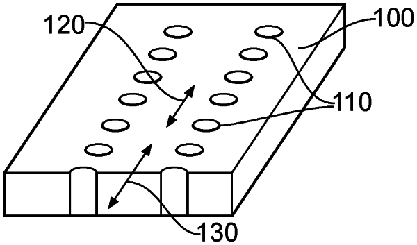
a planar substrate having conductive formations defining a substrate integrated waveguide test resonator, the test resonator comprising a three-dimensional region formed at least partly within the substrate having first and second planar conductive layers extending parallel to a plane of the substrate and one or more conductive sidewall formations perpendicular to the plane of the substrate defining a resonator side wall extending around the three-dimensional region,
wherein one planar conductive layer of the first and second planar conductive layers includes a test port comprising a conductive test connection electrically isolated from a rest of the one planar conductive layer, and
wherein the test port comprises an aperture formed in the one planar conductive layer, the conductive test connection being formed entirely within the aperture with a gap between the conductive test connection and the rest of the one planar conductive layer.
|