| CPC G01R 19/257 (2013.01) [G01R 19/2509 (2013.01); H03F 1/26 (2013.01); C12M 1/3407 (2013.01); G01N 27/301 (2013.01); H03F 2200/21 (2013.01); H03F 2200/504 (2013.01)] | 11 Claims |
|
1. A potential measurement device, comprising:
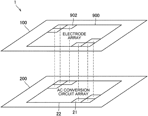
a first substrate having a plurality of read electrodes arranged in a two-dimensional array;
a second substrate on which the first substrate is stacked, wherein
each read electrode of the plurality of read electrodes is associated with one or more AD conversion circuits,
each AD conversion circuit of the one or more AD conversion circuits has independent correspondence to a read electrode of the plurality of read electrodes, and
at least a part of the one or more AD conversion circuits is arranged in a two-dimensional array on the second substrate; and
an amplifier circuit in a signal path from each read electrode of the plurality of read electrodes to each AD conversion circuit of the one or more AD conversion circuits.
|