| CPC G01N 27/4148 (2013.01) [G01N 27/4145 (2013.01); G01N 33/5438 (2013.01)] | 18 Claims |
|
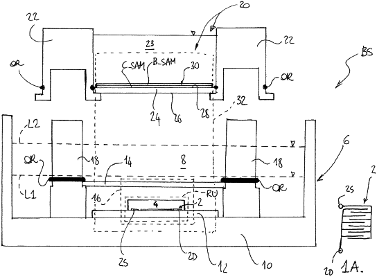
1. A field effect transistor (BS, BS′) sensor including:
a source-drain channel (2),
a semiconductor layer (4) on said source-drain channel (2),
a first gate electrode (14, 14′) arranged above said semiconductor layer (4),
a first well (6) enclosing said source-drain channel (2), said semiconductor layer (4) and said first gate electrode (14, 14′), the first well (6) being configured to be filled, in use, with a first liquid (8),
a second well (20) configured to be filled, in use, with a second liquid (23), the second well (20) being arranged above the first well (6), and
a second gate electrode (24, 24′) arranged above the first gate electrode (14, 14′) and exposed to an interior of the first well (6),
wherein the second gate electrode (24, 24′) provides at least a portion of a bottom wall of the second well (20).
|