| CPC G01B 7/20 (2013.01) [G01P 15/0922 (2013.01); H05K 7/026 (2013.01); H05K 7/1432 (2013.01)] | 9 Claims |
|
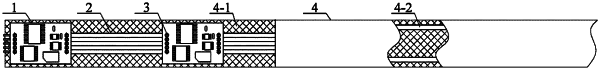
1. A packaging structure of a flexible sensing strip for monitoring large deformation at a deep position of a sliding mass, comprising a plurality of measurement unit modules and a stripped flat cable,
wherein each of the plurality of measurement unit modules comprises a printed circuit board (PCB) and electronic components, the electronic components being mounted on a front face of the PCB, the plurality of measurement unit modules are arranged at intervals in an extending direction of the stripped flat cable, the stripped flat cable is electrically connected to back faces of the plurality of PCBs in sequence to form a measurement unit cluster, the measurement unit cluster is packaged and molded by an extrusion technology of silica gel to form the flexible sensing strip, and the flexible sensing strip is capable of being wound into a sensing strip reel;
each of the plurality of measurement unit modules further comprises a plurality of pairs of interface bonding pads,
each pair of interface bonding pads being symmetrically mounted on a front face and a back face of the PCB, through holes penetrating positions, corresponding to each pair of interface bonding pads, of the PCB, each pair of interface bonding pads having consistent electric properties, and the stripped flat cable being electrically connected to the interface bonding pads.
|