| CPC B32B 3/02 (2013.01) [B32B 7/02 (2013.01); B32B 7/12 (2013.01); B32B 2307/7375 (2023.05); B32B 2457/20 (2013.01)] | 18 Claims |
|
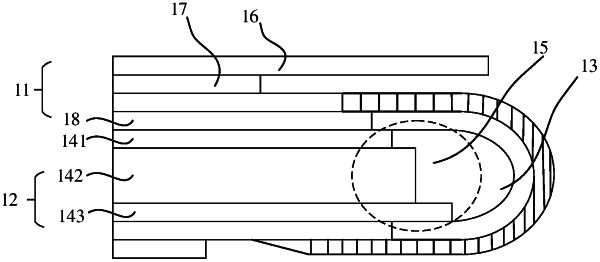
1. A display panel, comprising:
a bending region;
a first non-bending region;
a second non-bending region, the second non-bending region disposed opposite to the first non-bending region, and the second non-bending region connected to the first non-bending region through the bending region; and
a first support structure, the first support structure disposed between the first non-bending region and the second non-bending region, a step structure formed on a side of the first support structure near the bending region, and the step structure configured to support the bending region;
wherein the step structure comprises at least three step units arranged sequentially along a direction from the first non-bending region to the second non-bending region, or from the second non-bending region to the first non-bending region.
|