| CPC A61B 1/051 (2013.01) [A61B 1/0011 (2013.01); A61B 1/00124 (2013.01); A61B 1/0057 (2013.01); A61B 1/0676 (2013.01); H01L 27/14618 (2013.01); H01L 31/0203 (2013.01); H01L 31/02325 (2013.01); H01L 31/173 (2013.01); A61B 1/018 (2013.01)] | 12 Claims |
|
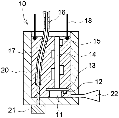
1. A packaged image sensor, comprising:
a substrate, including a first surface, a second surface opposite to the first surface, a through-hole, a plurality of first electric-conduction contacts, a plurality of second electric-conduction contacts, and a plurality of third electric-conduction contacts, wherein the plurality of second electric-conduction contacts and the plurality of third electric-conduction contacts are disposed on the first surface, the plurality of first electric-conduction contacts are disposed on the second surface, and the plurality of second electric-conduction contacts and the plurality of third electric-conduction contacts are electrically connected with the plurality of corresponding first electric-conduction contacts;
an image sensor, disposed on the substrate and electrically connected with the plurality of second electric-conduction contacts;
a light-emitting element, disposed on the substrate and near the image sensor and electrically connected with the plurality of third electric-conduction contacts; and
a first encapsulant, filled into a space between the image sensor and the light-emitting element with the through-hole of the substrate kept opened;
wherein a pipe is disposed inside the through-hole of the substrate and protruding from the second surface of the substrate where the first electric-conduction contacts are disposed.
|