| CPC H10N 70/231 (2023.02) [H10B 63/80 (2023.02); H10N 70/021 (2023.02); H10N 70/063 (2023.02); H10N 70/066 (2023.02); H10N 70/068 (2023.02); H10N 70/882 (2023.02); H10N 70/883 (2023.02)] | 22 Claims |
|
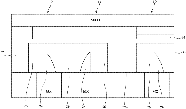
1. A device, comprising:
phase-change memory cells, each memory cell of the phase-change memory cells including:
a first element of a conductive material has a first surface opposite a second surface, the first surface contacts a second element of a phase-change material; and
a first insulating layer covers the first and second elements, the second surface of the first element is exposed from the first insulating layer;
a third element of a conductive material, an upper surface of the third element in contact with a lower surface of the second element; and
a second insulating layer surrounds the third element,
wherein the second element includes a vertical face extending from the upper face of the third element, the vertical face being in lateral contact with the first element.
|