US 12,004,405 B2
Display device and method of fabricating the same
Donghyun Lee, Asan-si (KR); and Si Joon Song, Suwon-si (KR)
Assigned to Samsung Display Co., Ltd., Yongin-si (KR)
Filed by SAMSUNG DISPLAY CO., LTD., Yongin-si (KR)
Filed on Nov. 23, 2022, as Appl. No. 18/058,724.
Application 18/058,724 is a continuation of application No. 17/363,834, filed on Jun. 30, 2021, granted, now 11,515,370.
Claims priority of application No. 10-2020-0131763 (KR), filed on Oct. 13, 2020.
Prior Publication US 2023/0088708 A1, Mar. 23, 2023
This patent is subject to a terminal disclaimer.
Int. Cl. G06F 3/044 (2006.01); G06F 3/041 (2006.01); H10K 59/40 (2023.01); H10K 71/00 (2023.01)
CPC H10K 59/40 (2023.02) [G06F 3/0412 (2013.01); G06F 3/0443 (2019.05); H10K 71/00 (2023.02)] 20 Claims
OG exemplary drawing
 
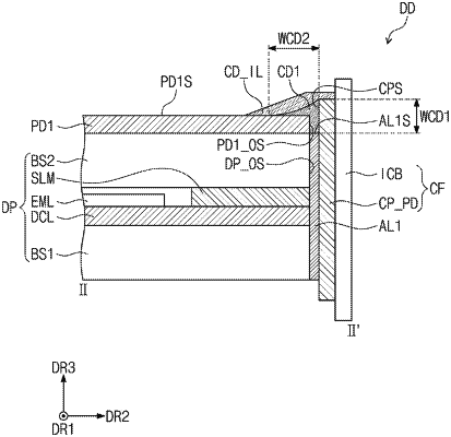
1. A display device comprising:
a display panel comprising a first substrate and a second substrate;
a first pad connected to a sensing electrode on the second substrate;
a first circuit film on a side surface of the display panel, electrically connected to the first pad, and comprising a first contact pad;
a first conductive layer electrically connecting the first pad to the first contact pad; and
a protection layer on the first conductive layer.