| CPC H10K 59/38 (2023.02) [H10K 59/131 (2023.02)] | 19 Claims |
|
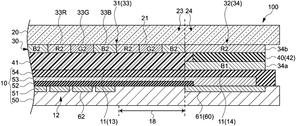
1. A display device, comprising:
an element substrate including a first surface, an organic EL element that emits light from a display region of the first surface, and peripheral wiring disposed to overlap in plan view with a peripheral region surrounding the display region;
a transparent substrate including a second surface facing the first surface;
a light shielding filter portion that includes a first color filter disposed in the peripheral region of the first surface and a second color filter disposed on the second surface to face the first color filter, and shields the peripheral wiring from light; and
a transparent adhesive layer that is provided between the first color filter and the second color filter and bonds the element substrate and the transparent substrate to each other.
|