| CPC H10K 59/353 (2023.02) [H10K 50/844 (2023.02); H10K 59/122 (2023.02); H10K 59/131 (2023.02); H10K 59/176 (2023.02); H10K 71/00 (2023.02); H10K 59/1201 (2023.02); H10K 2102/102 (2023.02); H10K 2102/103 (2023.02)] | 18 Claims |
|
1. A display panel, comprising:
a substrate;
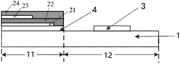
a plurality of sub-pixel regions disposed on the substrate, each of the sub-pixel regions comprising a first region and a second region, wherein the first region is provided with a buffer layer and a pixel circuit layer disposed on the substrate;
a first electrode, disposed on the substrate corresponding to the second region of each of the sub-pixel regions and directly contacting the substrate corresponding to the second region, wherein the second region comprises a light emitting area and a non-light emitting area, the first electrode is disposed on the light emitting area;
a lead, disposed on the substrate and comprising at least one of a scan line, a data line and a connection line disposed in the pixel circuit layer; and
an inorganic film layer, disposed on the substrate where a projection of the lead is overlapped and comprising at least one of a gate insulation layer, an interlayer insulation layer and the buffer layer.
|