| CPC H10K 59/131 (2023.02) [H10K 59/1213 (2023.02); H10K 59/123 (2023.02); H10K 59/124 (2023.02); H10K 71/00 (2023.02); H10K 59/1201 (2023.02); H10K 59/121 (2023.02)] | 20 Claims |
|
1. A display apparatus comprising:
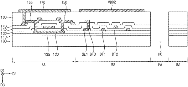
a substrate including a display area, a peripheral area surrounding the display area, a function-adding area, of which at least a portion is surrounded by the display area, and a detour area disposed between the display area and the function-adding area;
a plurality of pixel circuits disposed in the display area;
a plurality of data lines electrically connected to the pixel circuits and extending in a first direction in the display area;
a plurality of scan lines electrically connected to the pixel circuits, disposed under the data lines and extending in a second direction crossing the first direction in the display area; and
a plurality of detour lines disposed in the detour area,
wherein the detour lines includes:
a first detour line electrically connected to a first data line;
a second detour line electrically connected to a second data line and disposed in a different layer from the first detour line; and
a third detour line electrically connected to a first scan line and disposed in a different layer from the first scan line,
wherein at least one of the first detour line, the second detour line and the third detour line is disposed in a same layer as the data lines.
|