| CPC H10K 59/131 (2023.02) [H10K 59/35 (2023.02)] | 20 Claims |
|
1. A display apparatus comprising:
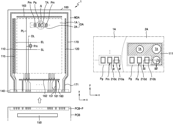
a substrate comprising a first area and a second area, wherein the second area includes a plurality of transmission areas;
main pixels on the first area, wherein each of the main pixels comprises a first pixel electrode, a first opposite electrode, and a first intermediate layer between the first pixel electrode and the first opposite electrode;
auxiliary pixels on the second area, wherein each of the auxiliary pixels comprises a second pixel electrode, a second opposite electrode, and a second intermediate layer between the second pixel electrode and the second opposite electrode;
a metal pattern layer on the second area and surrounding the plurality of transmission areas; and
an optical device under the substrate and corresponding to the second area, wherein the optical device overlaps with auxiliary pixels,
wherein the plurality of transmission areas are regions overlapping the substrate and corresponding to openings in the metal pattern layer, and
wherein the metal pattern layer surrounding the plurality of transmission areas is integrally formed.
|