| CPC H10K 59/126 (2023.02) [G09G 3/3233 (2013.01); H01L 27/1248 (2013.01); G09G 2300/0426 (2013.01); G09G 2300/0809 (2013.01); G09G 2320/0233 (2013.01)] | 20 Claims |
|
1. A display device, comprising a display panel,
the display panel comprises:
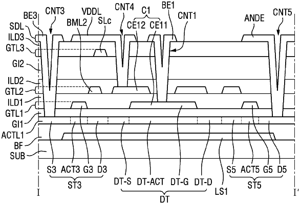
a plurality of first subpixels;
a first active layer disposed on a substrate and formed of a first material;
a first conductive layer disposed on the first active layer;
a second conductive layer disposed on the first conductive layer;
a second active layer disposed on the second conductive layer and formed of a second material different from the first material;
a third conductive layer disposed on the second active layer; and
a light-blocking layer disposed between the substrate and the first active layer and overlapping the first active layer in a thickness direction.
|