| CPC H10K 59/124 (2023.02) [H01L 27/1237 (2013.01); H10K 59/1213 (2023.02)] | 12 Claims |
|
1. A display apparatus, comprising:
a base substrate;
an active pattern disposed on the base substrate;
a gate insulation layer disposed on the active pattern;
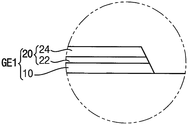
a gate electrode disposed on the gate insulation layer and overlapping the active pattern;
a first insulation layer disposed on the gate electrode and comprising silicon (Si), nitrogen (N), and hydrogen (H);
a second insulation layer disposed on the first insulation layer;
a storage electrode disposed between the first insulation layer and the second insulation layer and overlapping the gate electrode; and
a source electrode and a drain electrode which are disposed on the second insulation layer and are electrically connected to the active pattern,
wherein the first insulation layer has a total amount of hydrogen of about 5 atomic percent to about 30 atomic percent, Si—H bond in the first insulation layer is about 0.1 atomic percent to about 10 atomic percent, and the first insulation layer has a reflective index of about 1.884 to about 2.312.
|