| CPC H10K 59/1213 (2023.02) [G02F 1/136209 (2013.01); G02F 1/1368 (2013.01); H10K 59/1201 (2023.02); H10K 59/65 (2023.02)] | 20 Claims |
|
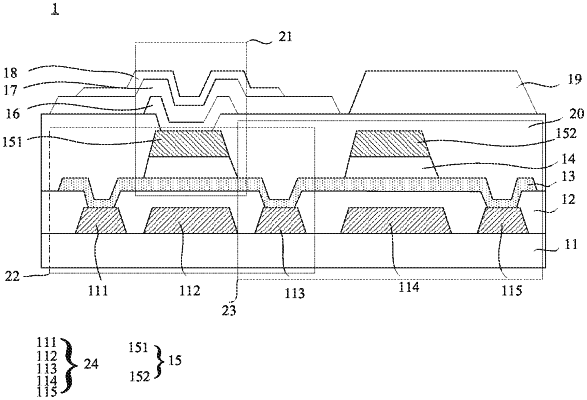
1. A display panel, comprising an array substrate, wherein the array substrate comprises:
a substrate;
a first gate disposed on one side of the substrate;
an active pattern disposed on one side of the first gate away from the substrate;
a second gate disposed on one side of the active pattern away from the first gate;
a photosensitive pattern disposed on one side of the second gate away from the active pattern; and
a polar plate disposed on one side of the photosensitive pattern away from the second gate;
wherein the array substrate further comprises a first source and a first drain, the first gate, the first source, the first drain, the second gate, and the active pattern form a first thin film transistor, and the second gate, the photosensitive pattern, and the polar plate form a capacitor.
|