| CPC H10K 50/858 (2023.02) [H10K 50/865 (2023.02); H10K 59/40 (2023.02); G06F 3/0412 (2013.01); H10K 59/122 (2023.02)] | 20 Claims |
|
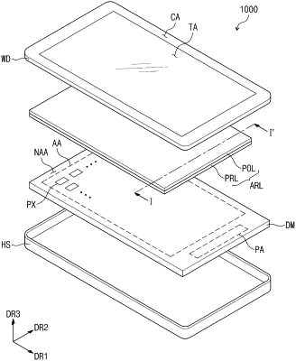
1. A display apparatus comprising:
a display layer including a plurality of organic light emitting elements and an encapsulation layer covering the plurality of organic light emitting elements, and defining a plurality of light emitting areas and a non-light emitting area surrounding the light emitting areas; and
an input sensing layer on the display layer,
wherein the input sensing layer comprises:
a first conductive pattern on the encapsulation layer;
an insulating layer on the first conductive pattern to cover the first conductive pattern, and defining a plurality of light collecting patterns overlapping with the light emitting areas in a plan view;
a second conductive pattern on a top surface of the insulating layer; and
an overcoat layer on the second conductive pattern to cover the insulating layer and the second conductive pattern,
wherein each of the light collecting patterns is recessed downward from the top surface of the insulating layer, and
wherein a portion of an upper surface of the encapsulation layer is exposed from the light collecting patterns and is covered by the overcoat layer.
|