| CPC H10K 50/844 (2023.02) [H10K 59/12 (2023.02); G09G 3/3275 (2013.01); G09G 3/3283 (2013.01); G09G 3/3291 (2013.01); G09G 2300/0408 (2013.01); H10K 59/122 (2023.02); H10K 59/124 (2023.02); H10K 77/111 (2023.02); H10K 2102/311 (2023.02); H10K 2102/361 (2023.02)] | 11 Claims |
|
1. A display device comprising:
a light emitting structure disposed on a substrate; and
a thin film encapsulation layer disposed on the light emitting structure and including an inorganic layer that contains silicon oxynitride and an organic layer,
wherein a portion of the inorganic layer has a stress intensity factor of about 1.6 MPa or more,
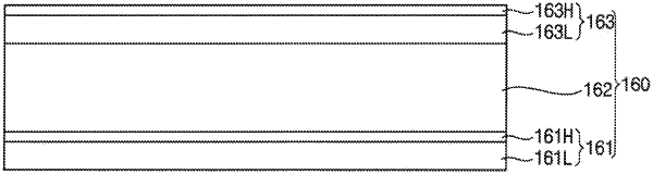
wherein the inorganic layer includes:
a first inorganic layer disposed between the light emitting structure and the organic layer and containing silicon oxynitride; and
a second inorganic layer disposed on the organic layer and containing silicon oxynitride,
wherein the first inorganic layer includes:
a first barrier layer contacting the organic layer; and
a second barrier layer contacting the light emitting structure,
wherein the first barrier layer is disposed between the organic layer and the second barrier layer, and
wherein a number of dangling bonds of the first barrier layer is less than a number of dangling bonds of the second barrier layer.
|