| CPC H10K 50/171 (2023.02) [H10K 50/15 (2023.02); H10K 50/16 (2023.02); H10K 59/12 (2023.02); H10K 59/40 (2023.02)] | 17 Claims |
|
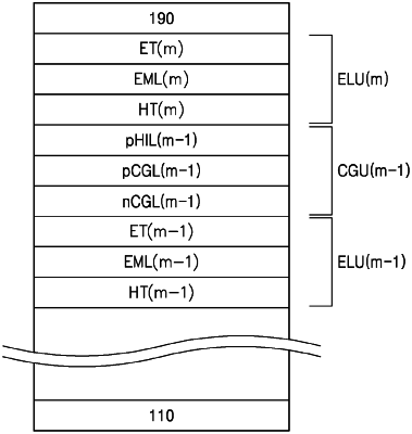
1. A light-emitting device comprising:
a first electrode;
a second electrode facing the first electrode; and
an organic layer between the first electrode and the second electrode,
wherein the organic layer includes a first emission layer, a second emission layer, and a charge generating unit between the first emission layer and the second emission layer,
the charge generating unit includes an n-type charge generating layer, a p-type charge generating layer, and a p-type hole injection layer,
wherein the n-type charge generating layer includes an n-type organic compound and a metal material,
the n-type organic compound includes a phenanthrene-based compound, a phosphine oxide-based compound and/or a phenanthroline-based compound,
the metal material includes at least one metal selected from an alkali metal, an alloy of an alkali metal, an alkaline earth metal, an alloy of an alkaline earth metal, a lanthanide metal, and an alloy of a lanthanide metal,
the p-type charge generating layer and the p-type hole injection layer each independently include an inorganic semiconductor material,
the inorganic semiconductor material included in the p-type charge generating layer and the inorganic semiconductor material included in the p-type hole injection layer each independently include a halide of a transition metal, a halide of a post-transition metal, bismuth, tellurium, a halide of bismuth, a sulfide of bismuth, a selenide of bismuth, a telluride of bismuth, a telluride of a transition metal, a telluride of a post-transition metal, a sulfide of a transition metal, a sulfide of a post-transition metal, a selenide of a transition metal, a selenide of a post-transition metal, or any combination thereof, and
the inorganic semiconductor material included in the p-type charge generating layer is substantially identical to or different from the inorganic semiconductor material included in the p-type hole injection layer.
|