| CPC H10K 50/15 (2023.02) [H10K 50/115 (2023.02); H10K 59/12 (2023.02); H10K 2102/331 (2023.02)] | 20 Claims |
|
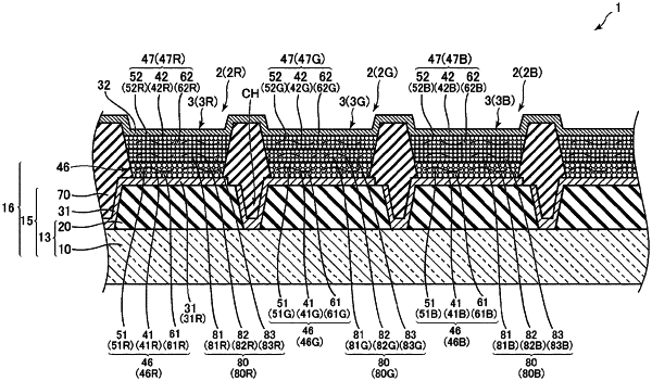
1. A display device comprising:
a first electrode;
a second electrode;
a light-emitting layer provided between the first electrode and the second electrode; and
a charge transport layer provided between the first electrode and the second electrode and containing a charge transport material configured to transport a charge to the light-emitting layer,
wherein at least one layer of the light-emitting layer and the charge transport layer is a function layer including a nanofiber and a photosensitive material.
|