| CPC H10B 61/00 (2023.02) [H01F 10/3254 (2013.01); H01F 10/3268 (2013.01); H01F 10/3286 (2013.01); H10N 50/10 (2023.02); H10N 50/80 (2023.02); H01F 10/329 (2013.01); H10N 50/85 (2023.02)] | 18 Claims |
|
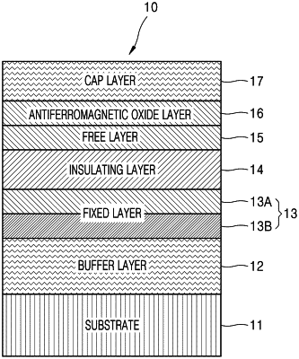
1. A magnetic tunnel junction element comprising:
a fixed layer maintaining a magnetization direction;
an insulating layer;
a free layer having a variable magnetization direction; and
an antiferromagnetic oxide layer in direct contact with the free layer, wherein
the fixed layer, the free layer, the insulating layer, and the antiferromagnetic oxide layer are sequentially stacked,
a thickness of the antiferromagnetic oxide layer is greater than or equal to about 0.5 nm and less than or equal to about 2 nm, and
wherein an electrical resistance of the antiferromagnetic oxide layer is less than an electrical resistance of the insulating layer.
|