| CPC H10B 43/40 (2023.02) [H01L 23/535 (2013.01); H10B 43/27 (2023.02)] | 20 Claims |
|
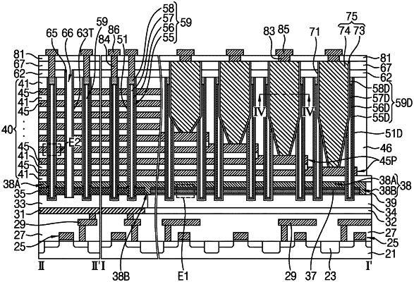
1. A semiconductor device comprising:
a substrate having a cell region and a connection region adjacent to the cell region;
a stacked structure in which a plurality of insulating layers and a plurality of electrode layers are alternately stacked on the substrate;
a source mold layer between the substrate and the stacked structure in the connection region;
an alternate conductive line between the substrate and the stacked structure in the cell region;
a plurality of cell channel structures in the cell region, the plurality of cell channel structures extending into the alternate conductive line while passing through the stacked structure;
a plurality of extension structures in the connection region, the plurality of extension structures extending into the source mold layer while passing through the stacked structure; and
a contact structure that is among the plurality of extension structures in the connection region while being in direct contact with one of the plurality of electrode layers,
wherein each of the plurality of cell channel structures comprises:
a channel pattern, and
an information storage pattern outside the channel pattern,
wherein the channel pattern is electrically connected to the alternate conductive line, and
wherein the plurality of extension structures are not electrically connected to the alternate conductive line.
|