| CPC H10B 43/27 (2023.02) [H10B 43/10 (2023.02); H10B 43/35 (2023.02); H10B 43/40 (2023.02); H10B 43/50 (2023.02); H01L 29/42344 (2013.01)] | 20 Claims |
|
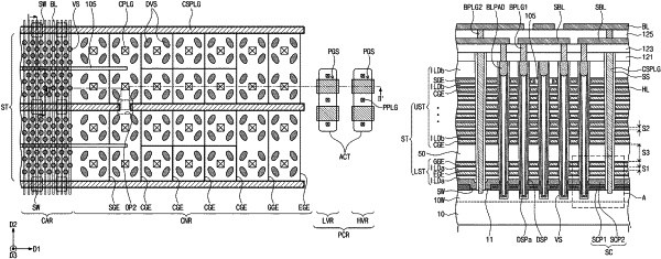
1. A three-dimensional (3D) semiconductor memory device, comprising:
a source structure on a substrate and extending in parallel to a top surface of the substrate; and
an electrode structure comprising an erase control gate electrode, a ground selection gate electrode, cell gate electrodes, and a string selection gate electrode, which are sequentially stacked on the source structure in a first direction that is perpendicular to the top surface of the substrate,
wherein the erase control gate electrode is a lowest one of the gate structure and has a first thickness in the first direction, the ground selection gate electrode is a second lowest one of the gate structure and has a second thickness in the first direction, a lowermost one of the cell gate electrodes is a third lowest one of the gate structure, and each of the cell gate electrodes has a third thickness in the first direction,
wherein the first thickness is greater than both the second thickness and the third thickness,
wherein the ground selection gate electrode is spaced apart from the erase control gate electrode by a first maximum distance and is spaced apart from the lowermost one of the cell gate electrodes by a second maximum distance in the first direction, and
wherein the second maximum distance is greater than the first maximum distance.
|