| CPC H10B 43/27 (2023.02) | 17 Claims |
|
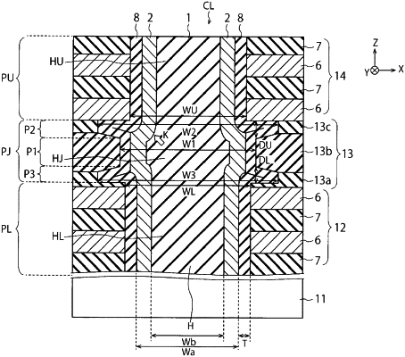
1. A semiconductor device, comprising:
a first stacked film including a plurality of first electrode layers separated from each other;
an insulating layer provided on the first stacked film;
a second stacked film provided on the insulating layer and including a plurality of second electrode layers separated from each other; and
a columnar portion including a first insulating film, a charge storage layer, a second insulating film, and a semiconductor layer, and extending along a first direction through the first stacked film, the insulating layer, and the second stacked film, wherein
the columnar portion extending in the insulating layer includes a first portion having a first width in a second direction intersecting the first direction, and a second portion provided at a different location along the first direction and having a second width in the second direction,
the columnar portion extending in the second stacked film includes a third portion having a third width along the second direction,
the second width is larger than the first width and the third width.
|