| CPC H10B 43/27 (2023.02) [H01L 23/5283 (2013.01); H10B 41/10 (2023.02); H10B 41/27 (2023.02); H10B 41/35 (2023.02); H10B 41/41 (2023.02); H10B 43/10 (2023.02); H10B 43/35 (2023.02); H10B 43/40 (2023.02)] | 19 Claims |

|
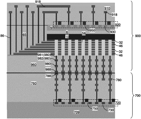
1. A bonded assembly comprising a memory die that is bonded to a logic die, wherein:
the memory die comprises:
a three-dimensional memory array located on a memory-side substrate;
memory-side dielectric material layers located on a first side of a combination of the three-dimensional memory array and the memory-side substrate;
memory-side metal interconnect structures and memory-side bonding pads embedded in the memory-side dielectric material layers;
a backside peripheral circuit comprising a first subset of logic devices configured to control operation of the three-dimensional memory array and located on a backside surface of the memory-side substrate;
backside dielectric material layers located on a second side of the combination of the three-dimensional memory array and the memory-side substrate that is an opposite side of the first side; and
backside metal interconnect structures that provide electrical connection between the three-dimensional memory array and the backside peripheral circuit embedded in the backside dielectric material layers; and
the logic die comprises:
a logic-side peripheral circuit comprising a second subset of the logic devices configured to control operation of the three-dimensional memory array and located on a logic-side substrate;
logic-side dielectric material layers located between the logic-side substrate and the memory die;
logic-side metal interconnect structures embedded in the logic-side dielectric material layers; and
logic-side bonding pads that are bonded to a respective one of the memory-side bonding pads and are embedded in the logic-side dielectric material layers,
wherein:
the three-dimensional memory array comprises an alternating stack of insulating layers and electrically conductive layers, memory openings vertically extending through the alternating stack, and memory opening fill structures located within the memory openings and comprising a respective vertical stack of memory elements; and
the alternating stack further comprises a staircase region in which all of the electrically conductive layers have variable lateral extents that decrease with a vertical distance from a horizontal plane including bonding surfaces of the memory-side bonding pads, wherein:
the first subset of logic devices comprises word line drivers configured to apply control voltages to the electrically conductive layers;
all of the word line drivers of the bonded assembly are located on the backside surface of the memory-side substrate and
the electrically conductive layers comprise word lines of the three-dimensional memory array.
|