| CPC H10B 43/27 (2023.02) [H01L 21/0217 (2013.01); H01L 21/02266 (2013.01); H01L 21/02274 (2013.01); H10B 41/27 (2023.02)] | 4 Claims |

|
1. A microelectronic device, comprising:
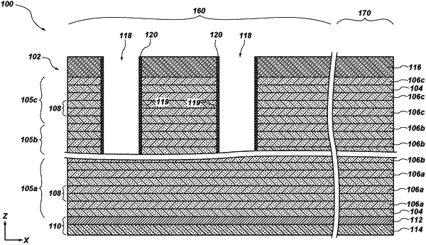
a stack structure including an array region and a peripheral region horizontally neighboring the array region, the stack structure comprising:
a first region comprising first levels respectively comprising:
silicon oxide material within the array region and the peripheral region;
within the array region, conductive material vertically adjacent the silicon oxide material; and
within the peripheral region, silicon nitride material vertically adjacent the silicon oxide material and having a first refractive index and a first ratio of nitrogen atoms to silicon atoms greater than about 1.60:1.00; and
a second region vertically overlying the first region and including second levels respectively comprising:
the silicon oxide material within the array region and the peripheral region;
within the array region, the conductive material vertically adjacent the silicon oxide material; and
within the peripheral region, additional silicon nitride material vertically adjacent the silicon oxide material, the additional silicon nitride material having a second refractive index greater than the first refractive index and having a second ratio of nitrogen atoms to silicon atoms less than about 1.60:1.00; and
a third region vertically overlying the second region and including third levels respectively comprising:
the silicon oxide material within the array region and the peripheral region;
within the array region, the conductive material vertically adjacent the silicon oxide material; and
within the peripheral region, the silicon nitride material vertically adjacent the silicon oxide material; and
strings of memory cells vertically extending through the stack structure and horizontally confined within the array region of the stack structure.
|