| CPC H10B 41/20 (2023.02) [H10B 41/35 (2023.02); H01L 21/02164 (2013.01); H01L 21/0217 (2013.01); H01L 21/022 (2013.01); H01L 21/02211 (2013.01); H01L 21/02274 (2013.01)] | 5 Claims |
|
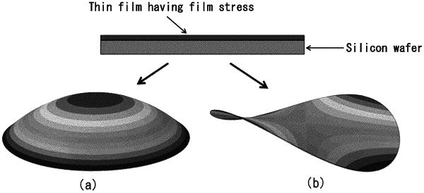
1. A method of reducing an amount of warp imparted to a silicon wafer having a (110) plane orientation and a <111> notch orientation by anisotropic film stress of a multilayer film that is to be formed on a surface of the silicon wafer, the method comprising:
forming the multilayer film on a surface of the silicon wafer in an orientation so that a direction in which the warp of imparted to the wafer will be greatest coincides with a direction in which Young's modulus of a crystal orientation of the silicon wafer is greatest.
|