| CPC H05K 3/181 (2013.01) [C23C 18/1605 (2013.01); C23C 18/165 (2013.01); C23C 18/20 (2013.01); C23C 18/32 (2013.01); C23C 18/38 (2013.01); H05K 1/032 (2013.01); H05K 2201/068 (2013.01)] | 13 Claims |

|
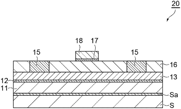
1. A method for manufacturing a wiring board, the method comprising, in a following order:
(a) a step of adsorbing an electroless plating catalyst to a first insulating material layer;
(b) a step of forming a metal layer on a surface of the first insulating material layer by electroless plating;
(c) a step of forming a resist having an opening for wiring pattern formation on a surface of the metal layer; and
(d) a step of forming a conductive part in a region, which is the surface of the metal layer and is exposed from the resist, by electrolytic plating, wherein
an arithmetic average roughness Ra of the surface of the first insulating material layer is 100 nm or less, and
a nickel content rate of the metal layer is 0.25 to 20% by mass.
|