| CPC H05K 3/064 (2013.01) [C23C 18/1646 (2013.01); C23C 18/1689 (2013.01); C23C 28/023 (2013.01); C25D 5/022 (2013.01); C25D 7/00 (2013.01); G03F 7/20 (2013.01); G03F 7/42 (2013.01); H05K 2203/072 (2013.01); H05K 2203/0723 (2013.01); H05K 2203/1152 (2013.01)] | 7 Claims |
|
1. A method for manufacturing a printed wiring board, comprising:
(a) providing an insulating substrate comprising a roughened surface, comprising
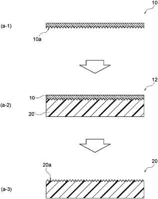
(a-1) providing a surface-treated copper foil having a treated surface having an arithmetic mean waviness Wa of 0.20 μm or more and 0.35 μm or less as measured in accordance with JIS B0601-2001 and a maximum height Sz of 3.0 μm or more and 4.0 μm or less as measured in accordance with ISO 25178,
(a-2) laminating an insulating substrate on the treated surface of the surface-treated copper foil to transfer a surface profile of the treated surface to a surface of the insulating substrate, and then
(a-3) etching away the surface-treated copper foil to obtain the insulating substrate comprising the roughened surface;
(b) performing electroless plating on the roughened surface of the insulating substrate to form an electroless plating layer less than 1.0 μm thick having a surface having an arithmetic mean waviness Wa of 0.10 μm or more and 0.25 μm or less as measured in accordance with JIS B0601-2001 and a kurtosis Sku of 2.0 or more and 3.5 or less as measured in accordance with ISO 25178;
(c) laminating a photoresist on the surface of the electroless plating layer;
(d) performing exposure and development on the photoresist to form a resist pattern;
(e) applying electroplating to the electroless plating layer via the resist pattern;
(f) stripping the resist pattern; and
(g) etching away an unnecessary portion of the electroless plating layer exposed by stripping of the resist pattern, to form a wiring pattern.
|