| CPC H05K 1/115 (2013.01) [H05K 1/0218 (2013.01); H05K 1/0265 (2013.01); H05K 1/0298 (2013.01); H05K 2201/0191 (2013.01); H05K 2201/096 (2013.01)] | 15 Claims |
|
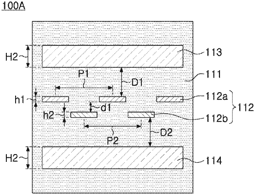
1. A printed circuit board comprising:
an insulating member;
a first wiring layer disposed in the insulating member, and including a first pattern layer and a second pattern layer spaced apart from each other based on a thickness direction of the printed circuit board;
a second wiring layer disposed in the insulating member, and spaced apart from the first pattern layer over the first pattern layer based on the thickness direction; and
a third wiring layer disposed in the insulating member, and spaced apart from the second pattern layer over the second pattern layer based on the thickness direction,
wherein, based on the thickness direction, an insulation distance between the first pattern layer and the second pattern layer is smaller than an insulation distance between the first pattern layer and the second wiring layer and an insulation distance between the second pattern layer and the third wiring layer, and
each of the first and second pattern layers is thinner than the second wiring layer and the third wiring layer.
|