| CPC H05K 1/0298 (2013.01) [H05K 1/115 (2013.01); H05K 1/144 (2013.01); H05K 3/4623 (2013.01); H05K 1/112 (2013.01); H05K 2201/096 (2013.01)] | 10 Claims |
|
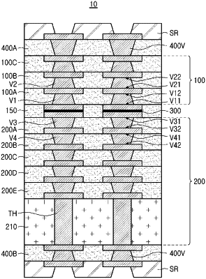
1. A printed circuit board comprising:
a first multilayer substrate including first and second vias adjacent to each other in a stacking direction of the printed circuit board;
a second multilayer substrate disposed on the first multilayer substrate in the stacking direction and including third and fourth vias adjacent to each other in the stacking direction;
an insulating layer arranged between the first and second multilayer substrates; and
an adhesive layer connecting respective one surfaces of the first and second multilayer substrates to each other,
wherein each of the first to fourth vias has a first surface and a second surface facing the first surface, the first surface being closer to the adhesive layer than the second surface, and the first surface having a larger transverse cross-sectional area than the second surface,
wherein the adhesive layer is disposed between a circuit pattern of the first multilayer substrate and a circuit pattern of the second multilayer substrate to connect the circuit pattern of the first multilayer substrate and the circuit pattern of the second multilayer substrate to each other,
wherein the adhesive layer has a side surface which is substantially coplanar with a side surface of at least one of the circuit pattern of the first multilayer substrate or the circuit pattern of the second multilayer substrate,
wherein the circuit pattern of the first multilayer substrate and the circuit pattern of the second multilayer substrate are embedded in the insulating layer, and
wherein the second multilayer substrate includes a core substrate having upper and lower surfaces such that more build-up layers are disposed between the insulating layer and the upper surface in the stacking direction than that disposed on the lower surface.
|