| CPC H05B 45/3725 (2020.01) [H05B 45/59 (2022.01)] | 15 Claims |
|
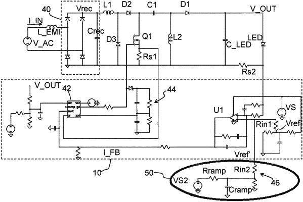
1. A driving circuit comprising:
a converter comprising:
an input to receive a supply voltage with a cyclic ripple having peak portions and valley portions;
a switch mode power converter circuit to convert the supply voltage, including an energy storage component and a main control switch;
an output; and
a current sensor for sensing an output current delivered at the output and generating a sensed current signal;
a control circuit to control a switching of the main control switch of the converter circuit, wherein the energy storage components is adapted to discharge to provide a regulated DC current at the output upon the switching of the main control switch; and
a modulation circuitry to apply a time-varying offset to the control circuit to modulate the regulated current thereby controlling the voltage across the energy storage component, wherein the modulation circuit comprises a ramp circuit for generating a time-varying ramp signal for combination with a static reference current signal to generate a modulated reference current signal and the control circuit comprises a comparator circuit for comparing the sensed current signal with the modulated reference current signal and an output of the comparator is for providing a current feedback signal for the control circuit so that the time-varying offset is adapted to ensure a margin of the voltage across the energy storage component above the supply voltage.
|