| CPC H04N 25/77 (2023.01) [H01L 27/146 (2013.01)] | 10 Claims |

|
1. An imaging device, comprising:
an imaging unit in which a plurality of shared sections each including two pixel regions adjacent at least in a first direction is provided and shared sections, of the plurality of shared sections, provided at closest positions in a second direction are disposed to shift in the first direction by one pixel region, the second direction intersecting the first direction;
a photoelectric converter provided for each of the two pixel regions;
an electric charge holding unit configured to hold signal charge generated by the photoelectric converter;
an electric charge voltage converter to which the signal charge is transferred from the electric charge holding unit;
a pixel transistor that is electrically coupled to the electric charge voltage converter, the pixel transistor being provided for each of the plurality of shared sections;
a semiconductor substrate provided with the photoelectric converter, the electric charge holding unit, and the electric charge voltage converter; and
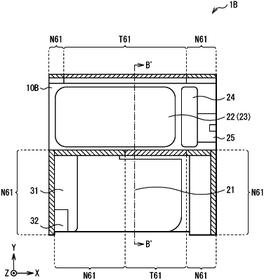
a first light shielding section provided between the photoelectric converter and the electric charge holding unit, wherein
the first light shielding section has a penetration region and a non-penetration region,
the penetration region is provided by penetration of the semiconductor substrate in a thickness direction, and
the non-penetration region is provided in a portion of the semiconductor substrate in the thickness direction.
|